Sony PlayStation PS4 Motherboard Diagram, PCB & Schematic
Sony PlayStation PS4: console mainboard schematics and boardview for component-level repair.
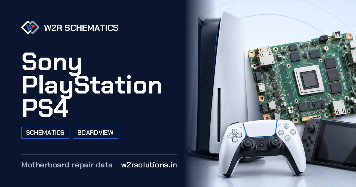
The Sony PlayStation PS4 is a home console mainboard that typically arrives at the repair shop with a malfunction. Upon receiving the board, the first step is to inspect the power input section.
Board Details
| Model | Sony PlayStation PS4 |
|---|---|
| Files | Schematic diagram · Boardview |
| Category | Gaming Console |
| Opens in | W2R Schematics desktop app (Windows 10 / 11) |
Common Sony PlayStation PS4 Repairs
Liquid and Physical Damage
Spill damage, corrosion and cracked parts.
Disc Drive
Disc drive connection and power faults on disc models.
No Video on HDMI
No picture, HDMI port damage and output faults.
Storage and Boot
Boot failures and storage faults.
Overheating and Fan
Heat shutdowns and the fan circuit.
Reading the Schematic
The schematic provides a detailed view of the board's components and their interconnections. By following a net, a technician can quickly identify the part referenced by its designator and begin diagnosis.
Where Faults Usually Start
The majority of faults that bring this board to the bench can be attributed to issues with the memory, storage, or power circuits. Faults in the HDMI output, USB ports, or network connectivity are also common.
How the Board Is Laid Out
The mainboard can be broadly divided into several areas: the processor section, the memory and storage section, the power circuitry section, and the cooling fan connector area. A technician will typically start by inspecting the processor section, then move on to the memory and storage section, and so on.
- The processor section includes the CPU, GPU, and other components that perform calculations and rendering.
- The memory and storage section houses the DRAM, flash memory, and other storage devices.
- The power circuitry section contains the voltage regulators, DC-DC converters, and other components that manage power distribution.
- The cooling fan connector area is responsible for circulating air and keeping the board at a safe operating temperature.
- A technician will also inspect the HDMI output, USB ports, and network connectivity components to identify any issues.
this board is a home console mainboard that typically arrives at the repair shop with a malfunction. The schematic, boardview, and PCB layout files for this board open in the W2R Schematics desktop app for Windows 10 and 11.
Sony PlayStation PS4 FAQ
Does W2R Schematics have the Sony PlayStation PS4 schematic diagram?
Yes. W2R Schematics has the Sony PlayStation PS4 schematic diagram, boardview and PCB layout. The files open in the W2R Schematics desktop app for Windows 10 and 11.
Can I find a component on the Sony PlayStation PS4 boardview?
Yes. In the W2R board viewer, right-click and choose Find Component or Find Net to highlight a part or signal on the Sony PlayStation PS4 board. When the schematic is linked to the board, double-clicking a net in the schematic highlights every pad on that net. Using the schematic and board together
Is the Sony PlayStation PS4 schematic free?
This page is free to read. The Sony PlayStation PS4 files open in the W2R Schematics app with a subscription. See plans and pricing
Also read: Sony PlayStation PS1 Schematics & Boardview
For similar diagnostics, refer to Sony PlayStation PS2 Schematics & Boardview.